LectureHistory of Transistor:The thermionic triode, a vacuum tube invented in 1907, propelled the electronics age forward, enabling amplified radio technology and long-distance telephony. The triode, however, was a fragile device that consumed a lot of power. Physicist Julius Edgar Lilienfeld filed a patent for a field-effect transistor (FET) in Canada in 1925, which was intended to be a solid-state replacement for the triode.
Lilienfeld also filed identical patents in the United States in 1926 and 1928. However, Lilienfeld did not publish any research articles about his devices nor did his patents cite any specific examples of a working prototype. Since the production of high-quality semiconductor materials was still decades away, Lilienfeld's solid-state amplifier ideas would not have found practical use in the 1920s and 1930s, even if such a device were built. In 1934, German inventor Oskar Heil patented a similar device. From November 17, 1947 to December 23, 1947, John Bardeen and Walter Brattain at AT&T's Bell Labs in the United States, performed experiments and observed that when two gold point contacts were applied to a crystal of germanium, a signal was produced with the output power greater than the input. Solid State Physics Group leader William Shockley saw the potential in this, and over the next few months worked to greatly expand the knowledge of semiconductors. The term transistor was coined by John R. Pierce as a portmanteau of the term "transfer resistor". According to Lillian Hoddeson and Vicki Daitch, authors of a biography of John Bardeen, Shockley had proposed that Bell Labs' first patent for a transistor should be based on the field-effect and that he be named as the inventor. |
|
Having unearthed Lilienfeld’s patents that went into obscurity years earlier, lawyers at Bell Labs advised against Shockley's proposal since the idea of a field-effect transistor which used an electric field as a “grid” was not new.
Instead, what Bardeen, Brattain, and Shockley invented in 1947 was the first bipolar point-contact transistor. In acknowledgement of this accomplishment, Shockley, Bardeen, and Brattain were jointly awarded the 1956 Nobel Prize in Physics "for their researches on semiconductors and their discovery of the transistor effect."
What is the transistor?
A transistor is a semiconductor device used to amplify and switch electronic signals and electrical power. It is composed of semiconductor material with at least three terminals for connection to an external circuit.
A voltage or current applied to one pair of the transistor's terminals changes the current flowing through another pair of terminals.
Because the controlled (output) power can be higher than the controlling (input) power, a transistor can amplify a signal.
Today, some transistors are packaged individually, but many more are found embedded in integrated circuits.
Types of transistor
Bipolar Junction Transistor:
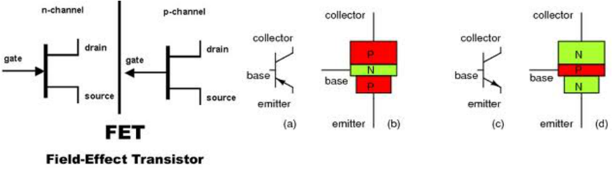
Bipolar transistors are so named because they conduct by using both majority and minority carriers. The bipolar junction transistor (BJT), the first type of transistor to be mass-produced, is a combination of two junction diodes, and is formed of either a thin layer of p-type semiconductor sandwiched between two n-type semiconductors (an n-p-n transistor), or a thin layer of n-type semiconductor sandwiched between two p-type semiconductors (a p-n-p transistor).
This construction produces two p-n junctions: a base–emitter junction and a base–collector junction, separated by a thin region of semiconductor known as the base region (two junction diodes wired together without sharing an intervening semiconducting region will not make a transistor).
The BJT has three terminals, corresponding to the three layers of semiconductor – an emitter, a base, and a collector. It is useful in amplifiers because the currents at the emitter and collector are controllable by a relatively small base current." In an NPN transistor operating in the active region, the emitter-base junction is forward biased (electrons and electron holes recombine at the junction), and electrons are injected into the base region.
Because the base is narrow, most of these electrons will diffuse into the reverse-biased (electrons and holes are formed at, and move away from the junction) base-collector junction and be swept into the collector; perhaps one-hundredth of the electrons will recombine in the base, which is the dominant mechanism in the base current.
By controlling the number of electrons that can leave the base, the number of electrons entering the collector can be controlled. Collector current is approximately β (common-emitter current gain) times the base current. It is typically greater than 100 for small-signal transistors but can be smaller in transistors designed for high-power applications.
Unlike the FET, the BJT is a low–input-impedance device. Also, as the base–emitter voltage (Vbe) is increased the base–emitter current and hence the collector–emitter current (Ice) increase exponentially according to the Shockley diode model and the Ebers-Moll model. Because of this exponential relationship, the BJT has a higher transconductance than the FET.
Bipolar transistors can be made to conduct by exposure to light, since absorption of photons in the base region generates a photocurrent that acts as a base current; the collector current is approximately β times the photocurrent. Devices designed for this purpose have a transparent window in the package and are called phototransistors.
Field-effect transistor:
The field-effect transistor (FET), sometimes called a unipolar transistor, uses either electrons (in N-channel FET) or holes (in P-channel FET) for conduction. The four terminals of the FET are named source, gate, drain, and body (substrate). On most FETs, the body is connected to the source inside the package, and this will be assumed for the following description.
In a FET, the drain-to-source current flows via a conducting channel that connects the source region to the drain region. The conductivity is varied by the electric field that is produced when a voltage is applied between the gate and source terminals; hence the current flowing between the drain and source is controlled by the voltage applied between the gate and source.
As the gate–source voltage (Vgs) is increased, the drain–source current (Ids) increases exponentially for Vgs below threshold, and then at a roughly quadratic rate ( Ids ᾳ (Vgs – VT )²) (where VT is the threshold voltage at which drain current begins) in the "space-charge-limited" region above threshold.
A quadratic behavior is not observed in modern devices, for example, at the 65 nm technology node.
For low noise at narrow bandwidth the higher input resistance of the FET is advantageous.
FETs are divided into two families: junction FET (JFET) and insulated gate FET (IGFET). The IGFET is more commonly known as a metal–oxide–semiconductor FET (MOSFET), reflecting its original construction from layers of metal (the gate), oxide (the insulation), and semiconductor. Unlike IGFETs, the JFET gate forms a p-n diode with the channel which lies between the source and drain.
Functionally, this makes the N-channel JFET the solid-state equivalent of the vacuum tube triode which, similarly, forms a diode between its grid and cathode. Also, both devices operate in the depletion mode, they both have a high input impedance, and they both conduct current under the control of an input voltage.
Metal–semiconductor FETs (MESFETs) are JFETs in which the reverse biased p-n junction is replaced by a metal–semiconductor junction. These, and the HEMTs (high electron mobility transistors, or HFETs), in which a two-dimensional electron gas with very high carrier mobility is used for charge transport, are especially suitable for use at very high frequencies (microwave frequencies; several GHz).
Unlike bipolar transistors, FETs do not inherently amplify a photocurrent. Nevertheless, there are ways to use them, especially JFETs, as light-sensitive devices, by exploiting the photocurrents in channel–gate or channel–body junctions.
FETs are further divided into depletion-mode and enhancement-mode types, depending on whether the channel is turned on or off with zero gate-to-source voltage. For enhancement mode, the channel is off at zero bias, and a gate potential can "enhance" the conduction. For depletion mode, the channel is on at zero bias, and a gate potential (of the opposite polarity) can "deplete" the channel, reducing conduction.
For either mode, a more positive gate voltage corresponds to a higher current for N-channel devices and a lower current for P-channel devices. Nearly all JFETs are depletion-mode as the diode junctions would forward bias and conduct if they were enhancement mode devices; most IGFETs are enhancement-mode types.
